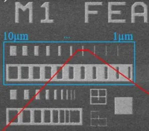
Regardless of its functionality, there is no IC-compatible process to pattern platinum. This can be attributed to the inertness of the noble metal. Pt survives extreme conditions, and is used in electrochemical, temperature, and gas sensors. In this paper, we introduce a process enabling Pt structures of 1 μm thickness and submicron feature size on 200mm wafers. It is the industry's first with focus on high process control while eliminating contamination issues. This is achieved by locally alloying the Pt with a sacrificial Al layer. The so-formed PtAl 2 is then removed by a selective wet-etch, which leaves a uniform Pt structure. The process is VLSI compatible, and can be adapted to any semiconductor fab to have a platinum processing capability. Pt as a third metal besides Al and Cu is a significant enabler for IC sensor technology.
https://ieeexplore.ieee.org/document/9117886
New Paper: Patterning Platinum by Selective Wet Etching of Sacrificial Pt-Al Alloy