Efficient Circuit Design for Time Discrete Analog Circuits
Clocked analog circuits are used very frequently in modern integrated circuit technology. There are inherently time discrete circuits and those that convert an actually continuous physical entity (such as voltage) into a time-discrete one by sampling, clocked charging or averaging.
Analog-to-digital converters (ADCs) are an example of discrete-time circuits that convert the continuous-magnitude voltage to a time discrete one by sampling. DC-DC converters map a continuous voltage back to a continuous voltage, but the conversion process uses a clocked operation. These converters therefore use a discrete-time control loop. Chopper amplifiers map a voltage difference to a voltage by clocked averaging. Phase-locked loops (PLLs) generate frequencies and measure the time between 2 edges. As such, they are inherently discrete-time circuits. Both frequency and edge spacing are time-discrete quantities. Treating them as a continuum creates problems in modeling [1-3], that are comparable to describing a pedestrian with a mobile phone, without considering that the pedestrian does not always look at the path.
A pedestrian who only looks up from his mobile phone every 2s cannot react to events every second.

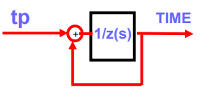
Comparable to this, in the case of a continuous description, an addition is approximated by an integration. With this approximation,
Although PLLs do not generate or measure any continuous variables, the control loop is modeled as a time-continuous system. This means that noise transfer functions cannot be determined correctly and are therefore not used in the circuit design to determine the requirements for the individual components, but only to explain the basic interaction.
If clocked modeling is used, then it is derived from continuous-time modelling [4-7]. This systematically excludes effects caused by the beat. Thus, continuous circuits have a turnaround time of 0. However, clocked systems have a turnaround time of N clock periods. However, at least one clock period.
This discrepancy is becoming more and more of a problem in modern CMOS processes as the clock frequencies for analog circuits increase.
The current approach to improving individual components without making a quantitative prediction about the potential for possible improvement is comparable to how bicycles were developed in the 1950s:
Sufficiently thick metal tubes were taken, a frame was welded from them and the moving parts were assembled. This worked well, the bike was just unnecessarily heavy and more material than necessary was used.
Later, a force diagram was drawn up and it was then possible to determine how thick the pipes had to be at which point. This enabled both material savings and the bicycle to be offered cheaper, as well as making it lighter.
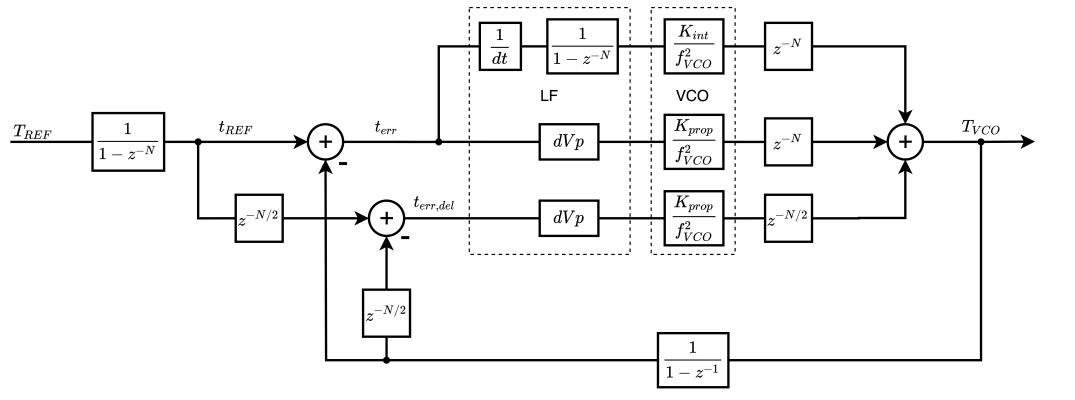
Applied to circuits, this means, for example, that instead of changing known circuits, known principles could be understood and expanded. Decoupling a principle from a block allows for a much deeper circuit understanding. For example, the integration of frequency to phase within a PLL does not take place in either the PFD or the VCO, but rather is done by looking at phase rather than frequency. This is comparable to looking at the distance traveled instead of the speed when driving a car. A look at how it works makes it possible to analyze parallels and differences between groups of circuits and to recognize the limits of common rules of thumb. The optimization of certain components could be placed under a cost-benefit analysis for the overall system. One could develop discrete-time circuits faster and with less experienced designers. In addition, chip area and power consumption would decrease.
Trustworthy modeling also enables the rapid evaluation of new concepts. Of course, this is not limited to PLLs, but applies to all clocked analog circuits. Instead of carrying out cost-intensive empirical experiments, the evaluation is already possible in the model. For example, you can already see in the model that 2 proportional paths have the same effect as one, even if they are time-shifted.
A general modeling approach for the circuit components and the system of a PLL (and later also other clocked circuits mentioned above) would enable a better and deeper understanding of these circuit classes for the purpose of optimization in application but also in teaching to train future circuit developers.
[1] D. Kim and S. Cho, "A hybrid PLL using low-power GRO-TDC for reduced in-band phase noise," IEEE Transactions on Circuits and Systems II: Express Briefs, vol. 66, no. 2, pp. 232-236, 2018.
[2] X. Gao, E. A. Klumperink, P. F. Geraedts, and B. Nauta, "Jitter analysis and a benchmarking figure-of-merit for phase-locked loops," IEEE Transactions on Circuits and Systems II: Express Briefs, vol. 56, no. 2, pp. 117-121, 2009.
[3] G. Urakawa, H. Kobayashi, J. Deguchi, and R. Fujimoto, "A Noise-Canceling Charge Pump for Area Efficient PLL Design," in 2020 IEEE International Symposium on Radio-Frequency Integration Technology (RFIT), 2020: IEEE, pp. 31-33.
[4] J. P. Hein and J. W. Scott, "z-domain model for discrete-time PLL's," IEEE transactions on Circuits and Systems, vol. 35, no. 11, pp. 1393-1400, 1988.
[5] B. Razavi, "zDomain Model for DiscreteTime PLL's," 1996.
[6] B. Razavi, Design of CMOS phase-locked loops: from circuit level to architecture level. Cambridge University Press, 2020.
[7] C.-H. Tsai, Z. Zong, F. Pepe, G. Mangraviti, J. Craninckx, and P. Wambacq, "Analysis of a 28-nm CMOS Fast-Lock Bang-Bang Digital PLL With 220-fs RMS Jitter for Millimeter-Wave Communication," IEEE Journal of Solid-State Circuits, vol. 55, no. 7, pp. 1854-1863, 2020.