Circuit boards characterization based on Transmission Line Pulsing (TLP)
Until recently, conversion of electrical energy to different voltage levels was mainly done with silicon based switching power electronic devices like power transistors or IGBTs. Using silicon as substrate leads to inherent limitations on essential properties for power electronics, like switching time of the electronic devices.Yet, faster switching times would lead to improved efficiency and smaller size of the converters.
With new technologies for power applications like GaN and SiC becoming widely available, new power systems utilizing these technologies have faster switching frequencies. However, using new technologies inside established solutions does not always lead to improvements. Parasitic effects of the boards and packages have much more prominent influences at the performance of power systems working at high switching frequencies. Until now, different methods characterize different parts of the system. For example, double pulse testing needs a complete power system and switching time tests require dedicated test circuits. Even established testing techniques like double pulse testing have to be adapted for the new materials.
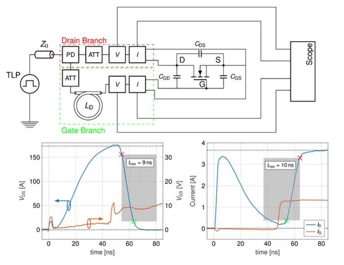
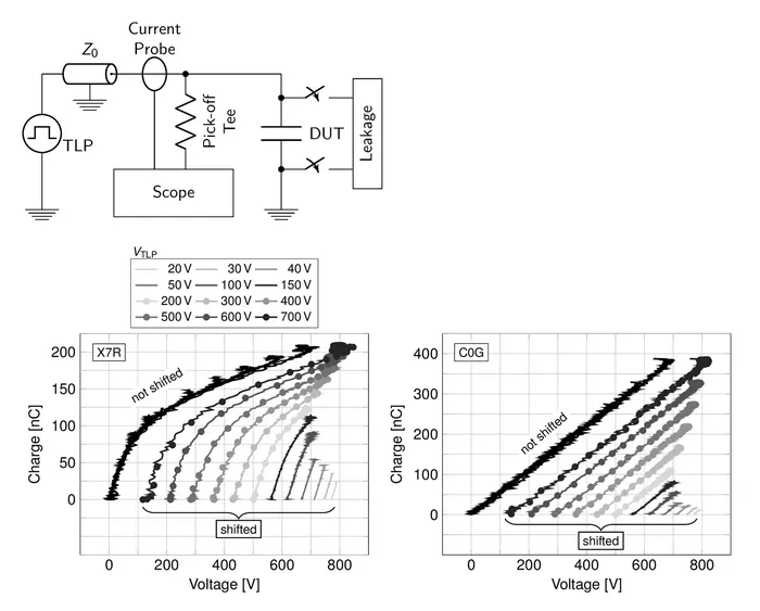
To overcome these obstacles, we are developing a single characterization method based on the Transmission Line Pulsing (TLP) technique, which is capable of extracting electrical properties of boards, devices and entire systems. The properties of the pulses (excitation):
- Amplitude (voltage source up to ±1500 V)
- Pulse length (2 ns to 1.5 µs)
- Risetime ≳ 0.2 ns (via rise time filter: up to 10 ns)
Advantages of the methodology:
- Large signal characteristic with sub-ns resolution
- Can be used on device level, wafer level and board level
- Active and passive elements can be characterized
- Transient characteristics can be extracted during the pulse:
- Capacitive behavior
- Inductive behavior, transformer coupling
- Switching characteristics

