Computation by 3D arrangements of nanomagnets
The year 2016 might mark a paradigm shift in digital computation as the well known \emph{laws} of transistor scaling seem to come to an end sooner as predicted. Hence, there is strong impetus for beyond CMOS device research in order to add new functionality to Integrated Circuits (ICs). The 2015 edition of the International Technology Roadmap for Semiconductors 2.0 -- Beyond CMOS, categorized current research on that field.
Our research group developed a promising technology --- the so-called perpendicular Nanomagnetic Logic (pNML)— over the last years. We aim to provide digital (Boolean) computation with non-volatile ferromagnetic computing states, purely powered and clocked by magnetic fields. Non-volatility combined with the capability of monolithic 3D integration in a planar fabrication process are key features. Instead of targeting CMOS substitution, additional functionality is provided by a co-processor architecture as a prospective back-end-of-line (BEOL) technology.
We envision a magnetic field clock for switching the computing elements by an on-chip inductor with soft-magnetic cladding to reduce the penalty of power consumption in the clocking field. The apparent unconventional computation in the ferromagnetic domain leads to highly dense computing structures with attojoule dissipation per bit operation and data-throughputs comparable to state-of-the-art high-performance CMOS CPUs. In appropriate applications with highly specialized computing architectures, they might even circumvent the bottleneck of time-consuming memory access, as non-volatile computing states and latches are inherently provided.
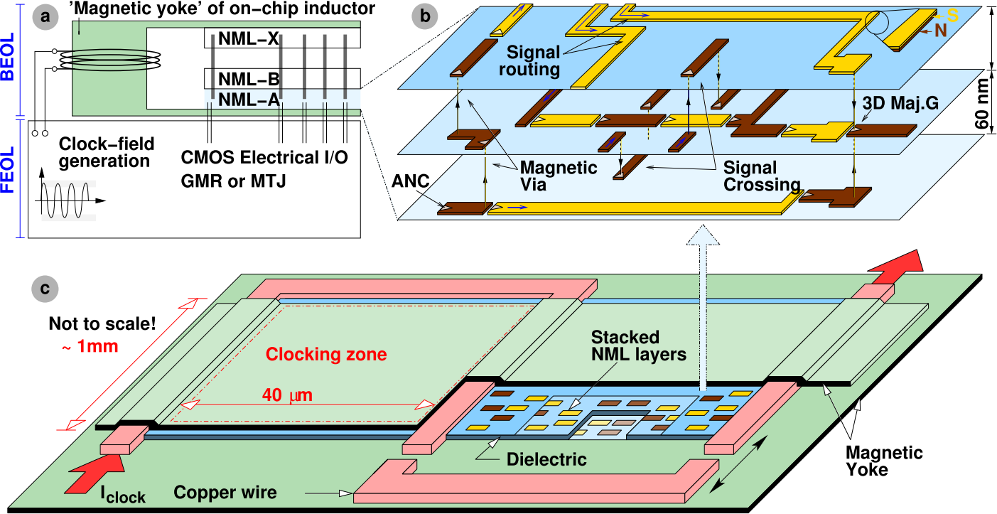
b) 3D arrangements of nanomagnets for computation and memory and
c) clocking zones to provide a magnetic field-clock to the pNML devices and circuits.
Becherer et al., Solid-State Electronics, 2016. DOI:10.1016/j.sse.2015.08.004
During the last years, we were able to design and construct several home-built measurement tools optimized for research on multilayer films with perpendicular magnetic anisotropy. We operate a laser magneto-optical Kerr-effect (MOKE) microscope and a wide-field
MOKE microscope with off-chip and on-chip magnetic field-pulsing capabilities down to the nanosecond range. Furthermore, a unique vector-field module for magnetic force microscopy (MFM) was developed and applied for domain imaging and in-situ characterization of pNML devices. Despite its capability to measure in 3D vector fields, the setup furthermore allows to directly integrate printed circuit boards for on-chip current pulses during MFM imaging.
The latest tool developed is a five target RF-magnetron sputtering tool illustrated below, partly funded within the DFG-project SCHM1478.9 with simultaneous (sequential) deposition of up to three materials (5 materials in multiplex mode) reducing downtime between the deposition of two layers, thus achieving higher-quality and more reproducible interfaces. It allows us to optimize film stacks with high throughput and full computer control. As the sputtering tool is optimized for small sample sizes, we can easily evaluate new materials with cost-effective 2’’ targets.
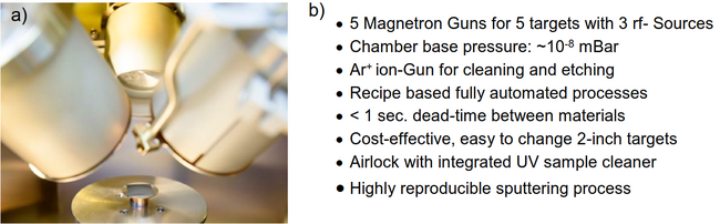
b) Table of merits of the sputtering tool incorporating 5 targets + 3 rf-generators for a fully automated sputtering process.
Funding and Duration
This project was mainly funded by Research grants of the German Science Foundation DFG
Completed projects
3D Integration of Nonvolatile Nanomagnetic Logic
https://gepris.dfg.de/gepris/projekt/114933698
Design of Circuits and Systems for Nonvolatile Nanomagnetic Logic
https://gepris.dfg.de/gepris/projekt/229838035
Cooperation Partners
Technische Universität München TUM
Chair of Nanoelectronics
Chair of Technical Electronics
Further Information
Principal Investigators: Markus Becherer, Doris Schmitt-Landsiedel, Paolo Lugli
Doctoral Candidates: Simon Mendisch
Press Releases and additional information
Field-coupled magnets could replace transistors in some computer chipsA new dimension for integrated circuits: 3D nanomagnetic logic
https://www.tum.de/nc/die-tum/aktuelles/pressemitteilungen/details/31824/
Irresistible Logic
https://portal.mytum.de/pressestelle/faszination-forschung/2015nr16/index_html
TEDxTUMSalon 2018 Using tiny magnets for computation
https://www.tedxtum.com/watch/markus-becherer/